Xiaojun Li
2025년 7월 7일
Can magnetron sputtering also deposit organic polymers such as polyimide? Drawing on an internal trial by VPI’s R&D team, this case study analyses—in five sections—how the SD-650MH high-vacuum magnetron sputtering system performs when polyimide is used as the target material. The discussion highlights the equipment’s strengths in low-power plasma ignition, high-vacuum stability and precise thickness control, together with its adaptability to sensitive targets and its operator-friendly design.
Case Study: Testing and Analysis of Polyimide Film Deposition with the SD-650MH Series High-Vacuum Magnetron Sputtering System
Polyimide (PI) is a high-performance polymer widely used in electronic devices and aerospace applications thanks to its outstanding heat resistance, electrical insulation and mechanical strength. Producing uniformly controlled ultrathin PI films in the laboratory, however, remains a challenge. Conventional wet-process coating tends to yield relatively thick layers that are hard to control precisely, while plasma polymerisation lacks stability and reproducibility at the nanometre scale. Magnetron sputtering, a mature physical-vapour-deposition (PVD) technique, is renowned for its stable, repeatable process, nanometre-level thickness control and excellent film uniformity—attributes long exploited for metal and inorganic coatings.
Can magnetron sputtering also deposit organic polymers such as polyimide? Drawing on an internal trial by VPI’s R&D team, this case study analyses—in five sections—how the SD-650MH high-vacuum magnetron sputtering system performs when polyimide is used as the target material. The discussion highlights the equipment’s strengths in low-power plasma ignition, high-vacuum stability and precise thickness control, together with its adaptability to sensitive targets and its operator-friendly design.
1 Effect of Sputtering Power on Film-Growth Rate
Sputtering power is a key parameter governing deposition rate and film quality. In this test, film-growth rate was measured under different power settings using radio-frequency (RF) magnetron sputtering—necessary because PI is an electrical insulator—with high-purity argon as the working gas.
Low-power ignition and plasma maintenance
The SD-650MH exhibits excellent low-power ignition capability. In an argon atmosphere of about 2–5 Pa, plasma was ignited successfully at only 1 W, producing a faint white glow with a slight pink tint (argon plasmas typically appear purplish). Gentle ignition minimises thermal shock and bombardment of the target, laying the foundation for stable sputtering.
Deposition rate at medium and high power
As power increased, the deposition rate rose almost linearly. Raising power from 20 W to 30 W boosted the observed rate from roughly 0.03–0.04 Å s⁻¹ to 0.05–0.06 Å s⁻¹ (1 Å s⁻¹ = 0.1 nm s⁻¹). Below about 20 W, thickness readings were erratic; only above this threshold did growth become measurable and controllable, indicating a minimum effective power is required for PI.
Overall, the SD-650MH permits finely tunable power output: it can ignite plasma at extremely low power yet maintain stable delivery in the medium-to-high range—ideal for identifying each material’s “power window”.
2 Sensitivity of the Polyimide Target
Polyimide presents two main challenges: out-gassing/thermal sensitivity and electrical insulation.
Out-gassing
A sharp rise in chamber pressure—from ~2 Pa to 6 Pa—was noted when power first reached 20 W, attributed to gases released as the PI target warmed. A stepped-power approach (pre-sputter at low power, then climb gradually) allowed gases to escape gently; subsequent runs showed no large pressure spikes. The system’s turbo-molecular and backing pumps quickly restored high vacuum, underscoring its ability to cope with organic out-gassing.
Insulating target requirements
Because PI is dielectric, RF sputtering is essential. The SD-650MH’s RF capability neutralises surface charge build-up and maintains a steady plasma, giving the system ample flexibility for “difficult” targets.
Plasma colour cues
A white glow tinged with pink was observed as sputtering progressed—likely PI fragments entering the discharge. A strong pink hue can warn of excessive target heating or decomposition, prompting operators to reduce power or raise argon flow.
Thus, water cooling, stepped-power ramping and RF supply collectively enable stable sputtering of sensitive polymer targets.
3 Thermal Management & Power-Ramping Strategy
Ion bombardment generates significant heat; controlling it is vital.
Efficient water cooling
A water-cooled cathode is standard on the SD-650MH. Even at 20–30 W, the PI target remained intact—no melting or charring—thanks to active cooling. Without it, target temperature could soar to thousands of degrees Celsius.
Low substrate heating
The system’s ring-shaped magnet array confines the plasma near the target, greatly reducing electron bombardment of the substrate. During the PI run, the substrate stage barely warmed—ideal for thermally sensitive wafers or flexible electronics.
Stepped power ramp
Plasma was ignited at 1 W, held at 5–10 W for pre-cleaning, then raised above 20 W for deposition. The RF supply’s smooth, stable output prevented current or voltage overshoot. Vacuum pumps responded instantly to pressure changes, and process windows from 0.5–5 Pa were explored. Optimum stability occurred around 1 Pa.
4 Operational Experience
Beyond hardware performance, the SD-650MH proved convenient and safe.
Rapid pump-down
From ambient to ~9 × 10⁻⁴ Pa in under 10 minutes; standby under vacuum further shortens turnaround.
Easy target & sample exchange
A top-opening chamber, standard 2-inch cathodes and quick-connect water lines enabled target swaps within minutes. The 150 mm rotating substrate stage ensured uniform thickness across multiple silicon wafers.
Touch-screen & PLC control
One-button pump-down, automatic sequencing and real-time readouts (pressure, power, thickness) minimise errors yet allow manual override. Interlocks prevent door opening under vacuum, and alarms shut down the system if coolant flow falters.
Maintenance
Long pump service intervals, anti-backstreaming features and a spacious chamber simplify cleaning. After PI deposition, only a faint brown ring near the target was visible; walls remained clean thanks to high vacuum and efficient pumping.
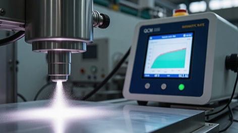
5 Film-Thickness Measurement & Data Stability
Thickness was monitored in situ with a quartz crystal microbalance (QCM).
Parameter set-up
Because PI was not in the library, density (1.5 g cm⁻³) and acoustic impedance (3.5 × 10⁵ cm s⁻¹) were estimated. Though absolute accuracy needs later calibration, relative trends are reliable.
Data behaviour
At low power/high pressure, rates fluctuated wildly (near the instrument’s resolution limit). Switching to ~1 Pa and ≥20 W stabilised readings: 0.03–0.06 Å s⁻¹ with ±0.01 Å s⁻¹ noise, mirroring theoretical linearity with power.
Post-run verification
A 25 W, 20-min run produced ~30 nm by QCM; a profilometer measured ~25–35 nm on the wafer—reasonable agreement confirming usability of the provisional PI parameters.
Reproducible thickness control lets users pre-set an end-point and shut down automatically—crucial for research repeatability.
Key Advantages Demonstrated
Outstanding low-power ignition (plasma lit at 1 W), protecting delicate targets and saving energy.
Fast, ultra-clean high vacuum (≤ 9 × 10⁻⁴ Pa in 10 min; ultimate ≤ 5 × 10⁻⁵ Pa) for high-purity films.
Nanometre-precision thickness monitoring with automatic end-point control.
Broad target compatibility—DC and RF sputtering support conductors, semiconductors and insulators alike.
Superior thermal design—water-cooled cathode and optimised magnetic circuit suppress target and substrate heating.
Operator-friendly automation and safety—touch-screen PLC control, interlocks, coolant and vacuum alarms, modular ports for future upgrades.
This study, conducted by VPI’s development and test team, confirms that the SD-650MH series is a reliable ally for challenging thin-film research—especially when working with sensitive materials such as polyimide. The team welcomes collaboration and discussion of customised sputtering solutions for specialised materials.