Engineer Wei
2026년 6월 8일
In the field of semiconductor thin-film fabrication, one phenomenon often appears in university laboratories, research institutes, and corporate R&D centers.
After a new high-vacuum magnetron sputtering system is installed, engineers and researchers usually do not start by fabricating the most complex device structures. Instead, they often begin with a seemingly ordinary material: copper (Cu).
Why Do Semiconductor Laboratories Often Start by Sputtering a Layer of Copper?Process Logic Behind Metal Seed Layers, Seen Through a Set of VPI Cu Thin-Film Experiments
In the field of semiconductor thin-film fabrication, one phenomenon often appears in university laboratories, research institutes, and corporate R&D centers.
After a new high-vacuum magnetron sputtering system is installed, engineers and researchers usually do not start by fabricating the most complex device structures. Instead, they often begin with a seemingly ordinary material: copper (Cu).
For those new to thin-film processing, this may seem surprising. After all, many research projects are not ultimately aimed at copper devices, and copper may not even be visible in the final product.
So why does the copper target appear so frequently in the first batch of laboratory samples?
The answer is simple.
For thin-film researchers, a copper film is not just a metal film. It is a “ruler” that can quickly indicate equipment status, process stability, and the feasibility of subsequent R&D work.
Copper Films Run Through Much of the Semiconductor Value Chain
If we look at modern semiconductor manufacturing, copper appears almost everywhere.
In advanced packaging, copper is an important part of RDL redistribution layers.In power devices, copper is widely used for electrodes and conductive layers.In MEMS devices, copper can serve as a conductive structure or functional layer.In sensor fabrication, copper is often used as a seed layer or intermediate conductive layer.In many research projects, copper is also one of the most common metal seed-layer materials.
Copper layers often serve as conductive layers, interconnects, electroplating precursor layers, or seed layers. A poor-quality copper film may directly affect all subsequent processes.
That is why many laboratories choose to start with copper when establishing a new thin-film process.
A Copper Film of Only Tens of Nanometers Is More Complex Than It Looks
Many people assume that copper film deposition is simple.
In fact, when the film thickness reaches several hundred nanometers, it is relatively easy to form a continuous conductive layer. But in the semiconductor industry, the more valuable copper films are often not 300 nm thick. They are only tens of nanometers thick, because seed layers usually operate within this thickness range.
When the copper film thickness is reduced to several tens of nanometers, many questions begin to appear:
Is the film continuous?Is the grain size uniform?Does the surface roughness meet the requirement?Is the adhesion sufficient?Is the resistivity stable?
These issues directly affect subsequent device performance.
For electroplating seed layers, insufficient copper film continuity may lead to non-uniform electroplating growth.For MEMS devices, poor adhesion may cause film peeling during later processing.For advanced packaging, excessive copper film resistivity can affect final electrical performance.
Therefore, in many semiconductor laboratories, researchers are not simply asking whether a copper film can be deposited. They are asking:
Under what process conditions can we obtain a copper film that meets the requirement?
A Set of VPI Cu Target Experiment Records
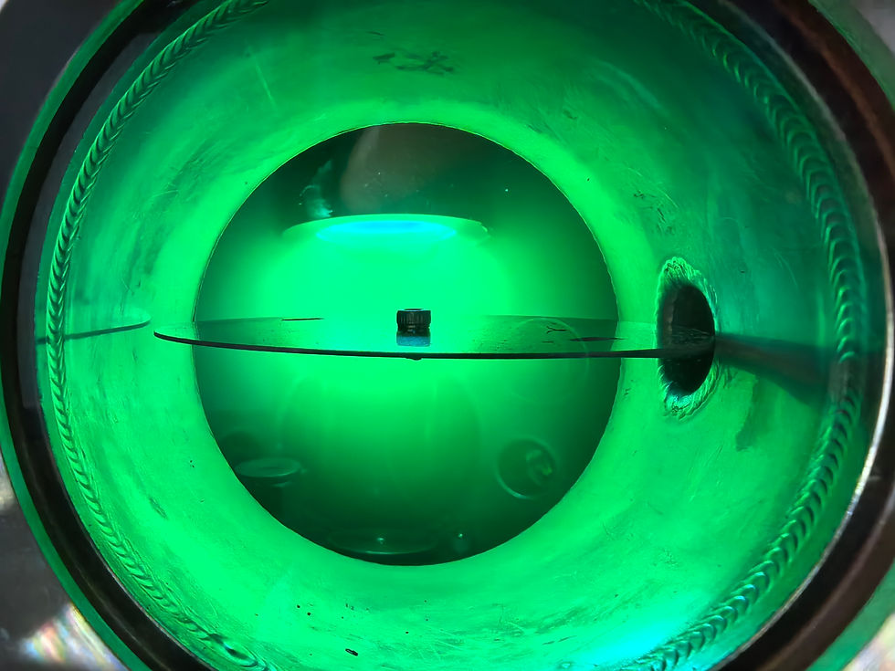
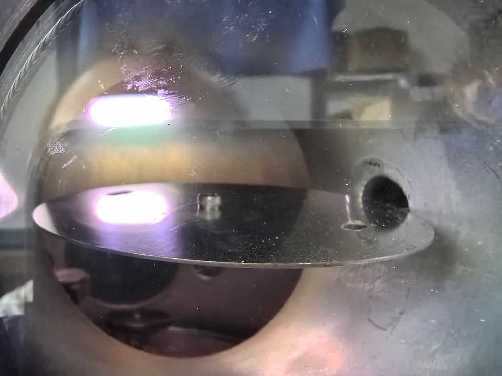
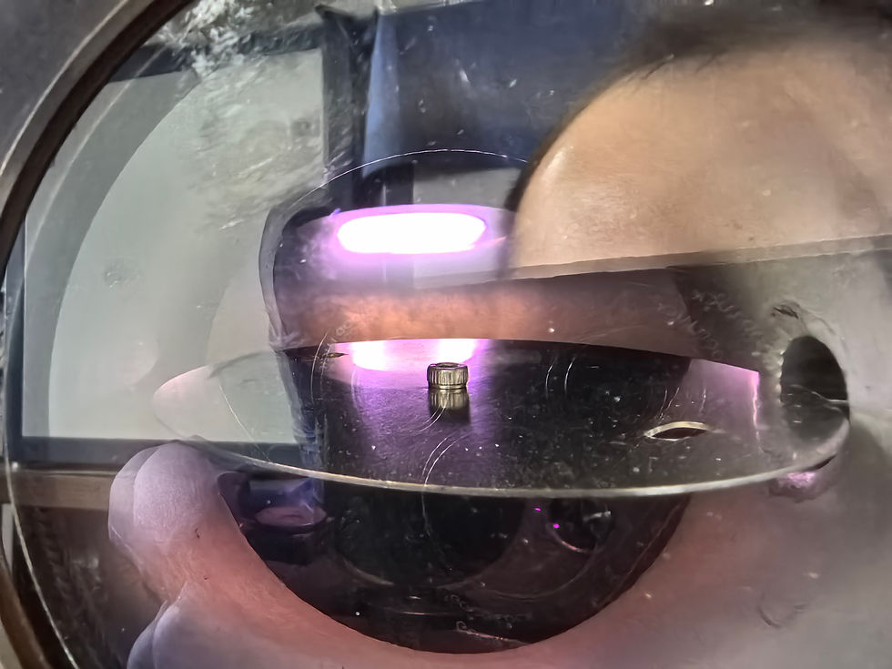
To establish a basic process database, VPI conducted high-vacuum magnetron sputtering experiments using a Cu target.
The experiment used:
2-inch Cu targetAr working atmosphereHigh-vacuum magnetron sputtering mode
The records show:
Pumping time: approximately 35 minutesVacuum environment: approximately 3.3 × 10^-3Working pressure: approximately 5 PaRecorded deposition rate: approximately 5-6 Å/s
Under the same process conditions, two representative deposition results were obtained:
Deposition Rate | Sputtering Time | Calculated Thickness |
5 Å/s | 1 min | approx. 30 nm |
6 Å/s | 4 min | approx. 144 nm |
For the semiconductor industry, these two thickness ranges are highly representative.
A thickness of around 30 nm falls within the typical seed-layer research range.A thickness above 100 nm gradually enters the range of stable conductive metal layers.
For this reason, many laboratories carry out follow-up tests around these thickness windows, including:
Film thickness measurementFour-point probe sheet resistance testingSEM surface morphology observationAdhesion testingSubsequent electroplating validation
These tests eventually form the laboratory’s own process database.
Behind the Copper Film Is the Capability of the Entire Process Platform
For researchers, the most important purpose of a copper film experiment is not simply to obtain a copper film.
It is to establish a reproducible process benchmark.
Once a copper film process has been verified, researchers can continue expanding toward more complex systems and various multilayer film structures.
At this point, the copper film acts like a ruler.
It helps the laboratory confirm equipment status, establish process windows, and calibrate key parameters. Real scientific innovation often grows gradually from these fundamental data points.
Starting From a Copper Target
In the semiconductor industry, many breakthroughs appear to come from complex devices, advanced structures, and precise design.
But once inside the laboratory, people often find that many research projects begin with the most fundamental materials.

Experimental Conditions Summary
Target: CuTarget specification: 2 inch, approximately 50 mm x 3 mmWorking gas: ArPumping time: approximately 35 minWorking pressure: 5 PaRecorded deposition rate: 5-6 Å/sRecorded film thickness: approximately 30 nm and 144 nm
The data in this article comes from VPI high-vacuum magnetron sputtering Cu target experiment records. Actual deposition results may vary depending on equipment configuration, power settings, target-substrate distance, substrate conditions, and measurement methods.